

Intro to GD-MS
Learn about Glow Discharge Mass Spectroscopy and discover how it can benefit your application
What is GD-MS
Glow Discharge Mass Spectrometry (GD-MS) is a powerful direct solid state elemental analysis technique that combines a glow discharge ion source with a magnetic sector mass spectrometer. This technique can quantify ultra-trace contaminants of virtually any element. It is ideal for analysing a range of materials, including high purity metals, superalloys, semiconductors and dielectrics.
Modern GD-MS systems are based on technology developed in the early 1970s, with the first commercial GD-MS systems launched in the 1980s. GD-MS systems fall into two categories: fast flow and low flow. This describes the flow rate of plasma gas used in the GD source. Typical flow rates for fast flow are around 500 sccm (standard cubic centimetres per minute), and low flow considerably lower at around 0.5 sccm. Whilst both techniques have their strengths, the Astrum uses a low flow source because of its superior user experience and performance in the most demanding applications, plus the lowest cost of ownership.
GD-MS uses a solid-state glow discharge source, generating ions directly from the sample surface. This eliminates the need for complex sample preparation, such as acid dissolution or lengthy processes that might introduce contamination. Just quick, clean, simple and safe sample introduction. Other elemental analysis techniques similar to GD-MS are Spark Optical Emission Spectroscopy (Spark-OES), Glow Discharge Optical Emission Spectroscopy(GD-OES) and Secondary ionisation Mass Spectrometry (SIMS)
How does GD-MS work?
A glow discharge ion source uses a low-pressure discharge gas in the presence of a high voltage gradient to create a steady plasma consisting of plasma gas and sample ions. The discharge gas of choice is typically argon due to its availability and high first ionisation energy, but low flow ion sources allow other gases, such as krypton and neon, to be used in specialist applications. Low flow GD-MS feature a cryogenically cooled source for ultimate stability, low gas backgrounds and to enable the analysis of low melting point materials such as Ga and In. Glow discharge sources operate on the following principle:
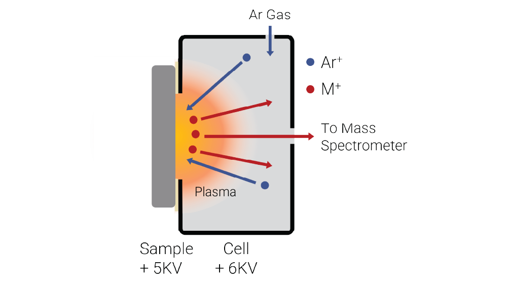
- A low-pressure plasma gas is introduced into the glow cell in the presence of a high voltage gradient (~1 kV). The sample is the cathode (+5 kV), and cell is the anode (+6 kV). Argon ions generated through electron impact and penning ionisation are accelerated towards the cathode.
- Upon impact, the ions remove particles from the surface of the sample in a process known as sputtering.
- The sputtered atoms are ionised in the plasma cloud.
- Electrostatic forces pull sample ions out of the cell, towards the extraction optics.
- Once outside the cell, the high positive potential of the cell (+6 kV) accelerates the sample ions towards the mass spectrometer.
- In the mass spectrometer, sample ions are separated based on their mass and charge ratio before quantification.
In the mass spectrometer, precision ion optics focus and shape the ion beam to enable the highest resolution for the best resolving power. A large electromagnet separates ions based on their mass and charge before quantification. GD-MS uses two detectors: a faraday cup for measuring high intensity signals, and a secondary electron multiplier for measuring the smallest signals from ultra-trace sample elements.
GD-MS is a high-resolution technique, capable of reaching resolving powers exceeding 10,000. This ensures most interferences are sufficiently resolved for accurate quantification. Interferences can arise from many sources, with notable examples including CNO-based polyatomics, multiply charged species, and plasma-gas based species. The resolution in GD-MS is primarily controlled by directing the beam through two narrow apertures, one at the source and one at the collector end of the instrument, the source slit and collector slit respectively. These may have fixed or variable width, ranging ~1 mm to <10 µm.
Tuning is performed with the collector slit open on a flat top peak at ~300RP to maximise ion transmission. Following this, the collector slit is closed to produce a narrow beam, giving a pointed, higher resolution peak. The peak shape is optimised for the highest resolution using the mass spectrometers’ ion optics. Typical tuning routines take <5 minutes, with some higher resolution operating conditions taking a little longer to complete. Most analyses are performed at ~4000 RP: this is the optimum balance between good signal intensity and resolution, since increasing RP usually reduces signal intensity.
GD-MS & GD-OES Products

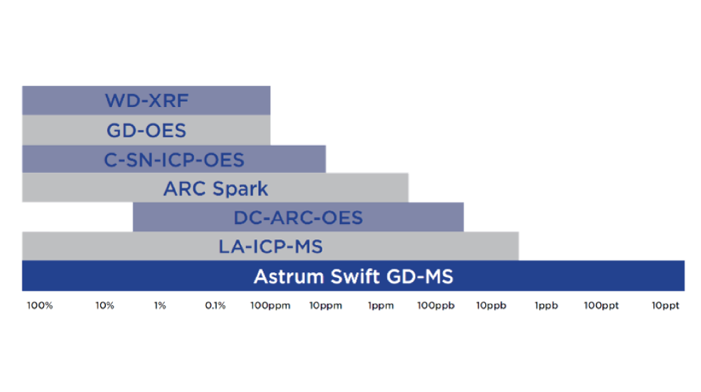
Quantify virtually all elements from 100% to sub-ppb in a single scan, with a dynamic range across 12 orders of magnitude.

From our sister company SPECTRO: fast measurements and high throughput for alloy elements using arc/spark OES.

From our sister company SPECTRO: industry’s best-selling arc/spark optical emission spectrometry (OES) analyzer.

From our sister company SPECTRO: compact, affordable, and ideal for routine analysis of elemental content in metals.

From our sister company SPECTRO: The arc/spark mobile metal analyzer for precise analysis without compromise.

From our sister company SPECTRO: portable metal analyzer applies more advanced OES technology.

GD-MS
Advantages
- Quantify virtually all elements in the periodic table, including C, N, O, Cl and other light elements. Cryo-cooled low-flow instruments exhibit an especially low gas background, as standard.
- Absolute matrix matched calibration standards are not necessary – use a standard RSF calibration or similar matrix materials for data with exceptional accuracy.
- Low cost per analysis: For low flow source instruments especially, minimal gas usage, high sample throughput, and few consumables mean minimal running costs, Plus, reusable source components last indefinitely.
- High throughput, up to 5 full elemental analyses per hour, with sub-ppm detection limits.
- Wide dynamic range spanning 12 orders of magnitude (100% to sub-ppb).
- Depth profiling capability with nm resolution.

GD-MS
Sample Types
There are two formats for GD-MS samples, pin and flat:
- Pin samples made from wire or cut materials. 1 – 3 mm ø x 22 mm
- Flat samples, with at last one flat side for analysis. 10 – 40 mm Ø x 20 mm
The design of the source enables flexible sample geometries to suit any given application. Powders, aggregates, wires, filaments, turnings are all possible. Binder and support materials are all possible methods to enable analysis.
Non-conductive samples can also be analysed by using a secondary cathode to support glow discharge. This simple sample preparation step uses a high purity conductive material, such as In or Ta, to facilitate glow discharge and sputtering of non-conductive materials.
Applications
High Purity Metals
Elemental metals with purities ranging 3N (99.9 %) to 7N (99.99999 %). This application strongly benefits from the wide dynamic range, low gas background and flexible sample geometry. Typical examples include Al, Cu, In, Ta, Ga, W, Ti, etc.

Applications
Advanced Alloys & Superalloys
Complex advanced alloy materials for use in extreme environments or safety critical applications, such as aerospace & defence. These materials must meet strict QC standards, often featuring sub-ppm concentration limits on certain elements. The technique’s high throughput, high precision and high resolution enable precise and rapid turnaround when efficiency is paramount. Typical examples include Inconel, Hastelloy, Réne alloys, precious metal catalysts, etc.

Applications
Semiconductor Materials
Elemental and compound materials used in semiconductor devices, including dielectrics, with purities ranging 3N (99.9 %) to 7N (99.99999 %). These benefit from non-conducting materials analysis (see secondary cathode analyses) and ultra-low detection limits. Typical examples include GaAs, Si, SiC, InP, CZT, etc.
GD-MS Analyses
GD-MS is a powerful and customisable technique that allows a user to refine analysis conditions to suit their application. For example, ultra-high purity materials benefit from higher signal intensity, enabling lower limits of detection (LOD). For these applications, particularly where interferences are minimal, high resolution is not always required, and a user may wish to operate at ~3000 RP and higher ion transmission, lowering LODs. Conversely, for a complex alloy sample, interferences can be significant. In these applications, purity requirements are often less demanding, and higher resolution will help a user distinguish between interference signals and analyte signals – here it may be useful to tune the instrument to >4000 RP at the cost of some signal loss.
In addition to resolution and LODs, GD-MS allows users to optimise their analysis routines in numerous other ways, allowing for refinements including analysis time/sample throughput, sample pre-sputtering and source temperature. Adjusting these parameters gives the best control and enables GD-MS to seamlessly integrate into their workflow.
Applications
GD-MS is an industrial high precision, solid-state analytical technique optimised for the elemental analysis of critical materials. It excels in applications ranging from high purity metals and semiconductors to superalloys analysis.
.svg%3Fh%3D32%26iar%3D0%26w%3D32&w=64&q=75)
Dielectrics
Direct solid analysis of non-conducting materials with ultra-trace impurity detection in advanced dielectric materials used in high-performance electronic devices.
.svg%3Fh%3D32%26iar%3D0%26w%3D32&w=64&q=75)
Semiconductor
Ultimate detection limits enable the characterisation of ultra-high-purity materials at the 6N and 7N level, providing confidence in material qualification and process control.
.svg%3Fh%3D32%26iar%3D0%26w%3D32&w=64&q=75)
Superalloys
Rapid multi-element analysis supports high-throughput quality control, ensuring compositional consistency in safety-critical components.
.svg%3Fh%3D32%26iar%3D0%26w%3D32&w=64&q=75)
Metals
Exceptional sensitivity enables ultra-trace impurity detection in high-purity metals, supporting reliability, yield and performance in demanding manufacturing applications.
Industry
Material Sciences
GD‑MS is a valuable tool for materials science because it provides direct solid-state elemental analysis with ultra-trace detection limits across most of the periodic table. Researchers and manufacturers can accurately characterise the purity and composition of metals, alloys, semiconductors, and advanced materials without complex sample preparation. Its wide dynamic range, high sensitivity, and depth profiling capabilities help support materials development, quality control, process optimisation, and failure analysis, enabling greater confidence in material performance and reliability.
Industry
Semiconductor
The Astrum Swift delivers ultra-trace elemental analysis for compound semiconductor materials such as CdTe and GaAs, where impurity control is critical to device performance and manufacturing yield. Ultimate detection limits enable the characterisation of up to 7N purity materials. By identifying trace metallic contaminants at extremely low concentrations, the Astrum Swift provides confidence in materials qualification, process control and the production of high-performance semiconductor devices.
Applications and Articles on GD-MS
